Edited by Bill Travis
Colm Slattery, Analog Devices, Limerick, Ireland -- EDN , 2/20/2003
Many applications require low-frequency signal generators that can deliver high-performance, high-resolution signals. This Design Idea presents a circuit that generates frequencies of 0 to 1 MHz. Sinusoidal, triangular, and square-wave outputs are available. You can achieve frequency resolution of better than 0.1 Hz and phase resolution of better than 0.1°; thus, you can program exact coherent frequencies. This feature is useful in digital modulation and frequency-tuning applications. The circuit uses the ADµC831 and AD9834 to generate the required frequencies (Figure 1). You can program the microcontroller from either a PC or a Unix-based workstation. You then program the AD9834 using a three-wire serial interface via the microcontroller. The interface word is 16 bits long.
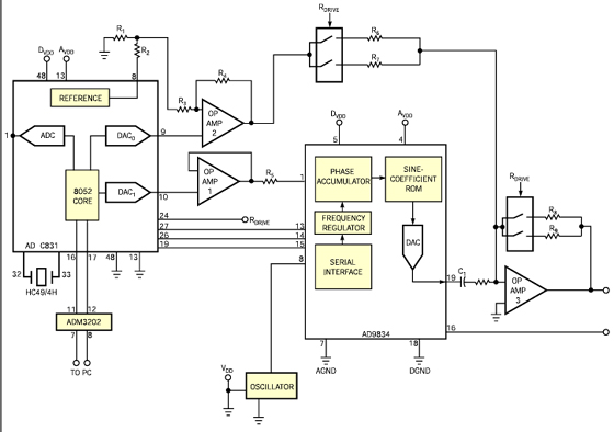
Figure 1
You can program the AD9834 to provide sinusoidal, triangular, and square-wave outputs using the DDS (direct-digital-synthesis) architecture. The chip operates as an NCO (numerically controlled oscillator) using an on-chip, 28-bit phase accumulator, sine-coefficient ROM, and a 10-bit D/A converter. You typically consider sine waves in terms of their magnitude form, A(t)=sin(ωt). The amplitude is nonlinear and is, therefore, difficult to generate. The angular information, on the other hand, is perfectly linear. That is, the phase angle rotates through a fixed angle for each unit in time. Knowing that the phase of a sine wave is linear, and, given a reference interval (clock period), you can determine the phase rotation for that period: ΔPhase=ω dt; ω=ΔPhase/dt=2πf, and f=(ΔPhase×fMCLK)/(2π), where dt=1/fMCLK, and fMCLK is the master clock.
Using this formula, you can generate output frequencies, knowing the phase and master-clock frequency. The phase accumulator provides the 28-bit linear phase. The amplitude coefficients of the output sine wave are stored in digital format in the sine-coefficient ROM. The DAC converts the sine wave to the analog domain. If you bypass the ROM, the AD9834 delivers triangular waveforms instead of sinusoidal waveforms. A square-wave output is also available on the part. As shown in Figure 1, the sinusoidal/ triangular output waveforms are available on the IOUT pin (Pin 19); and the square wave output is available on the SIGN_BIT_OUT pin (Pin 16). You program the DDS by writing to the frequency registers. The analog output from the part is then: fOUT=fMCLK/228×(frequency-register word).
The outputs of the DDS have 28-bit resolution, so effective frequency steps on the order of 0.1 Hz are possible to a maximum of approximately 1 MHz. Two phase registers are available that allow 12-bit phase resolution. These registers phase-shift the signal by: Phase
shift=2π/4096×(phase-register word).
A 50-MHz crystal oscillator provides the reference clock for the DDS. The output stage of the DDS is a current-output DAC loaded by an external resistor. A 200Ω resistor generates the required peak-to-peak voltage range. The output is ac-coupled through capacitor C1. The MicroConverter contains two on-chip, 12-bit DACs. DAC1 varies the current through R5, adjusting the full-scale current of the DDS via the FSADJUST pin. The equation to control the full-scale current of the DDS DAC is: IOUT (full-scale)=18×I×R5.
DAC0, the internal reference of the MicroConverter, and op amp 2 allow for offset control of the output voltage of the DDS. You can program this dc offset to ±10V at 10-bit resolution. When R1=R2 and the gain of op amp 2=8, then the output of op amp 2 is: VOUT=(DAC output–(VREF/2))×8, yielding a ±10V range.
Resistors R6 through R9 allow for control of gain through op amp 3. The gain of the op amp is a function of resistor switching, which you enable using the RDRIVE pin available on the MicroConverter. This operation allows for an effective programmable-output amplitude of approximately ±10V p-p. Thus, the circuit allows for programmable sinusoidal and triangular waves, including dc offsets, and the ability to set peak-to-peak amplitude of approximately ±10V. The square wave output on the SIGN_BIT_OUT pin has 0 to 5V amplitude. For low-frequency operation, a lowpass filter normally serves to filter reference-clock frequencies, spurs, and other images. For
 applications in which the output signal needs amplification, you should use a narrowband filter to filter out unwanted noise before the gain stage. A third-order filter would be good enough to remove most of the unwanted noise. Applications for this circuit range from signal-waveform generation to digital modulation. You can use the system in frequency-sweeping and -scanning applications and in resonance applications that use the frequency as an excitation signal to determine circuit resonance. Another useful application is as a reference oscillator for a DLL system.