摘 要
本文聚焦于基于28nm工艺的CMOS低压低功耗压控振荡器(VCO)的电路与版图设计。随着集成电路技术的不断发展,低功耗、高性能的VCO在无线通信、时钟生成等领域扮演着至关重要的角色。本文旨在设计一款满足特定参数要求的VCO,包括电源电压为1.8V,频率调谐范围为2.5GHz至3.1GHz,以及工作电流小于10mA。
首先,根据设计指标及CMOS电路特点,本文详细分析了VCO的基本工作原理,并绘制了相应的电路原理图。通过Candence Spectre仿真工具,对电路进行了深入的仿真分析,以评估电路的性能指标与元器件参数之间的关系。这一过程对于指导后续的版图设计至关重要。
在版图设计方面,本文采用了先进的版图设计技术,根据仿真分析得出的元器件参数,精确设计了各元件的版图几何尺寸以及工艺参数。为了确保版图设计的正确性,本文还进行了详细的DRC(设计规则检查)和LVS(版图与电路图一致性检查)验证。
此外,本文还探讨了从性能指标到版图设计的优化路径。通过反复仿真、修改和验证,不断优化设计方案,以确保最终设计的VCO能够满足所有参数要求,并具备优良的性能。
综上所述,本文成功设计了一款基于28nm CMOS工艺的低压低功耗压控振荡器,并完成了相应的版图设计。该设计不仅满足了特定的参数要求,还为后续的集成电路制造提供了可靠的设计基础。
关键词:28nm CMOS;低压低功耗;压控振荡器;电路设计;版图设计;Candence Spectre仿真
ABSTRACT
This paper focuses on the circuit and layout design of CMOS low-voltage and low-power pressure-controlled oscillator (VCO) based on 28nm process. With the continuous development of integrated circuit technology, low power consumption, VCO with high performance plays a vital role in wireless communication, clock generation and other fields. The purpose of this paper is to design a VCO that meets the requirements of specific parameters, including a supply voltage of 1.8V, a frequency tuning range of 2.5GHz to 3.1GHz, and an operating current of less than 10 mA.
Firstly, according to the design index and CMOS circuit characteristics, this paper analyzes the basic working principle of VCO in detail, and draws the corresponding circuit schematic diagram. A thorough simulation analysis of the circuit is conducted to evaluate the relationship between the performance index of the circuit and the component parameters. This process is critical to guiding the subsequent layout design.
In terms of layout design, this paper adopts the advanced layout design technology, according to the simulation analysis of the component parameters, accurately designed the layout geometric size and process parameters of each component. In order to ensure the correctness of layout design, detailed DRC (design rule check) and LVS (map and circuit diagram consistency check) verification are also conducted.
Furthermore, the optimization path from performance metrics to landscape design. Through repeated simulation, modification and verification, the design scheme is continuously optimized to ensure that the final design VCO can meet all parameter requirements and have excellent performance.
In conclusion, this paper has successfully designed a low pressure and low power pressure-controlled oscillator based on 28nm CMOS process, and completed the corresponding layout design. This design not only meets the specific parameter requirements, but also provides a reliable design basis for the subsequent IC manufacturing.
Key words: 28nm CMOS; low voltage low power consumption; voltage controlled oscillator; circuit design; layout design; Candence Spectre simulation
目 录
前 言 5
第1章 绪论
1.1 课题背景
1.1.1 研究背景
1.1.2研究内容
1.2 电路设计流程
1.3 主要工作以及任务分配
1.3.1主要工作
1.3.2 任务分配
第2章 版图基础知识
2.1 版图的设计简介
2.1.1 版图的概念
2.1.2 版图中层的意义
2.2 CMOS工艺技术
2.2.1概述
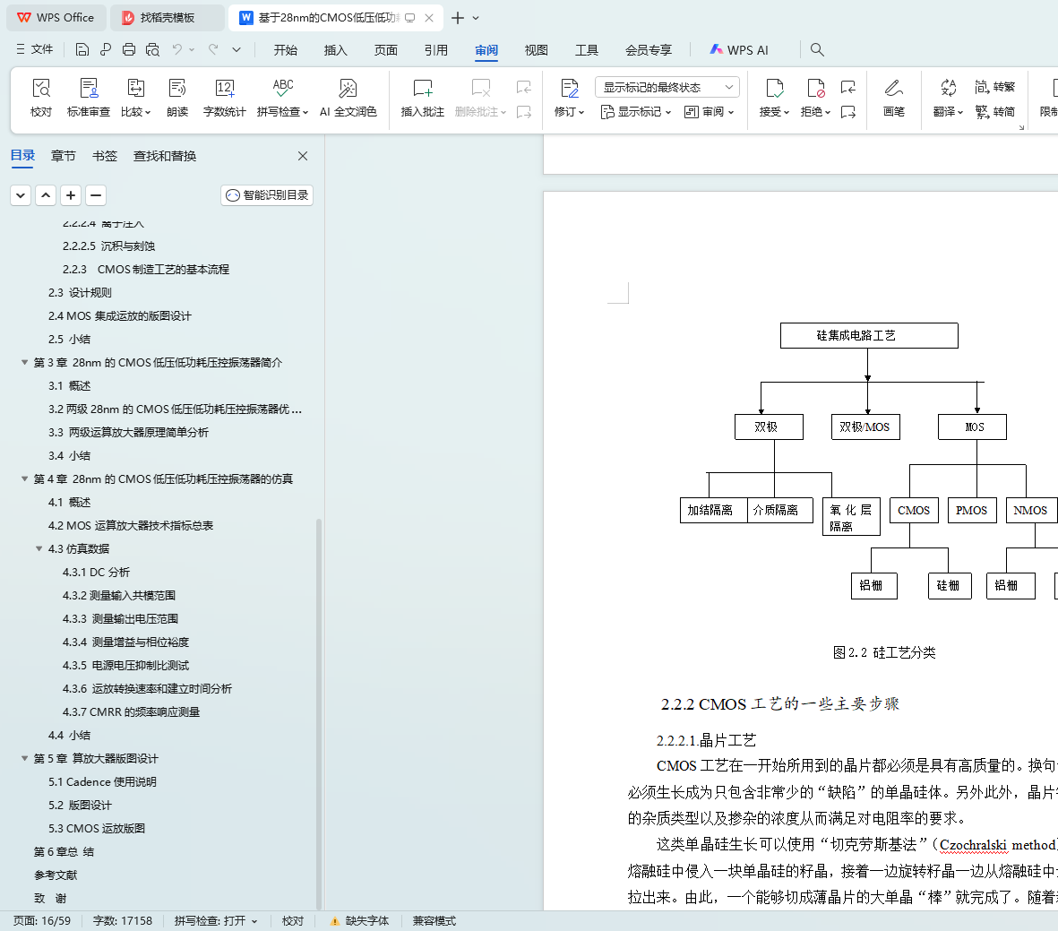
2.2.2 CMOS工艺的一些主要步骤
2.2.3 CMOS制造工艺的基本流程
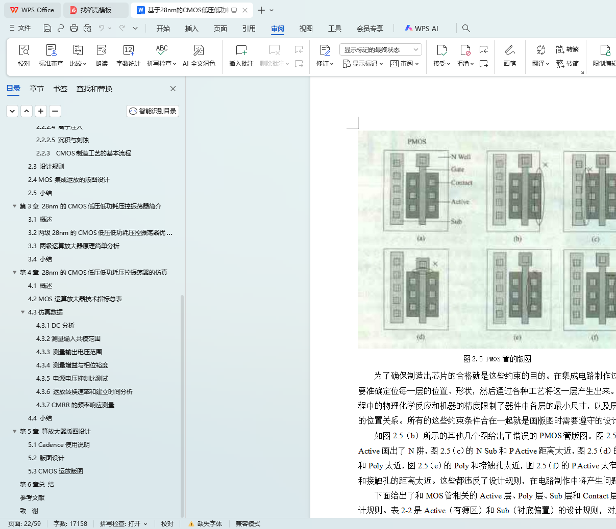
2.3 设计规则
2.4 MOS集成运放的版图设计
第3章 28nm的CMOS低压低功耗压控振荡器简介
3.1 概述
3.2两级28nm的CMOS低压低功耗压控振荡器的优点
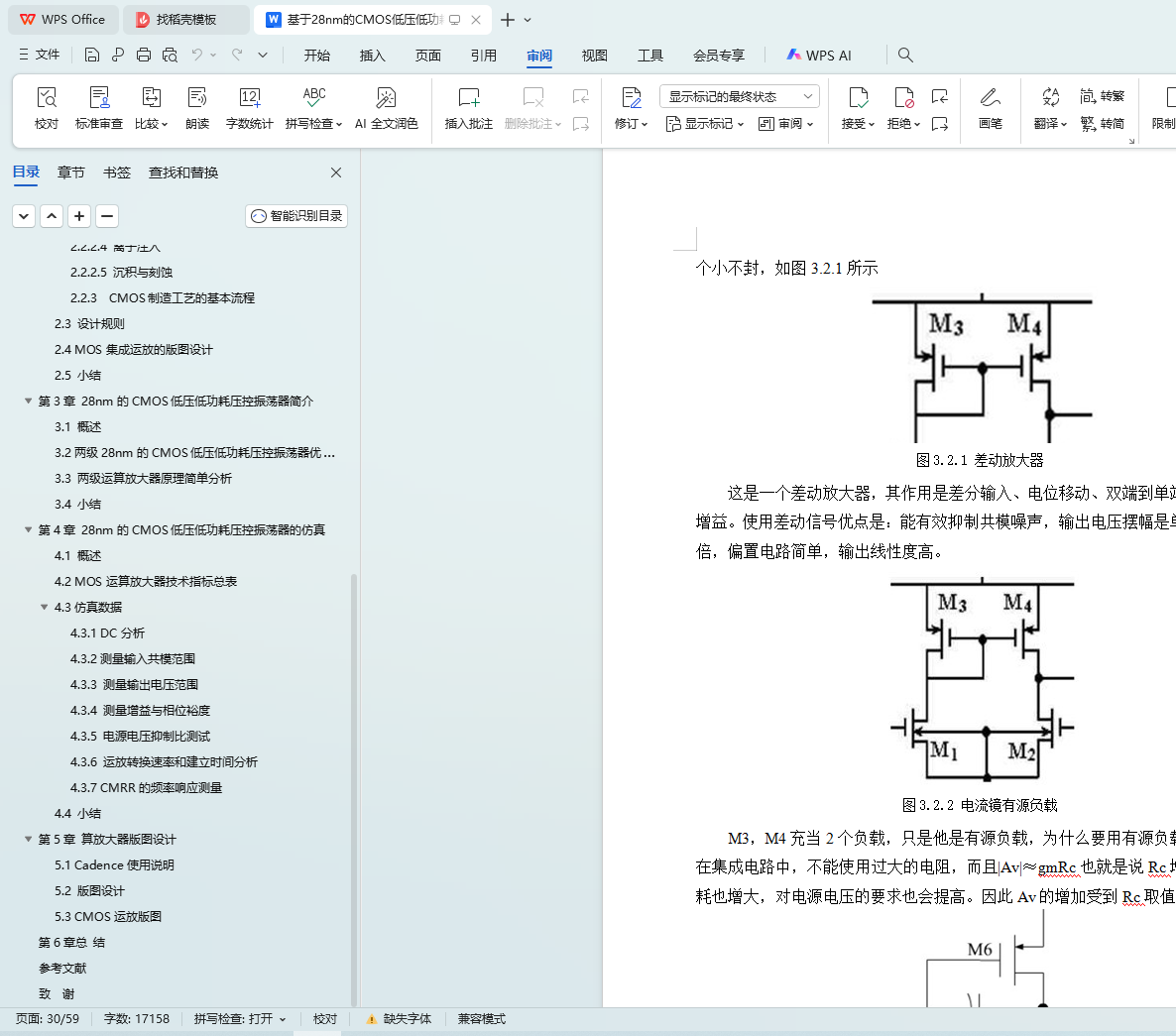
3.3 两级运算放大器原理简单分析
第4章 28nm的CMOS低压低功耗压控振荡器的仿真
4.1 概述
4.2 MOS运算放大器技术指标总表
4.3仿真数据
4.3.1 DC分析
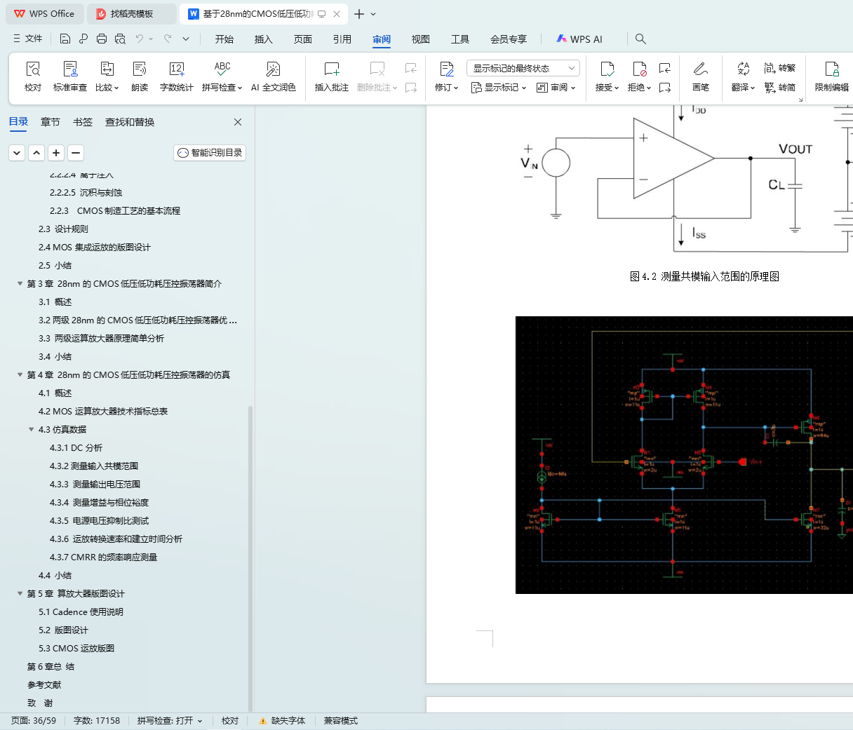
4.3.2测量输入共模范围
4.3.3 测量输出电压范围
4.3.4 测量增益与相位裕度
4.3.5 电源电压抑制比测试
4.3.6 运放转换速率和建立时间分析
4.3.7 CMRR的频率响应测量
第5章 算放大器版图设计
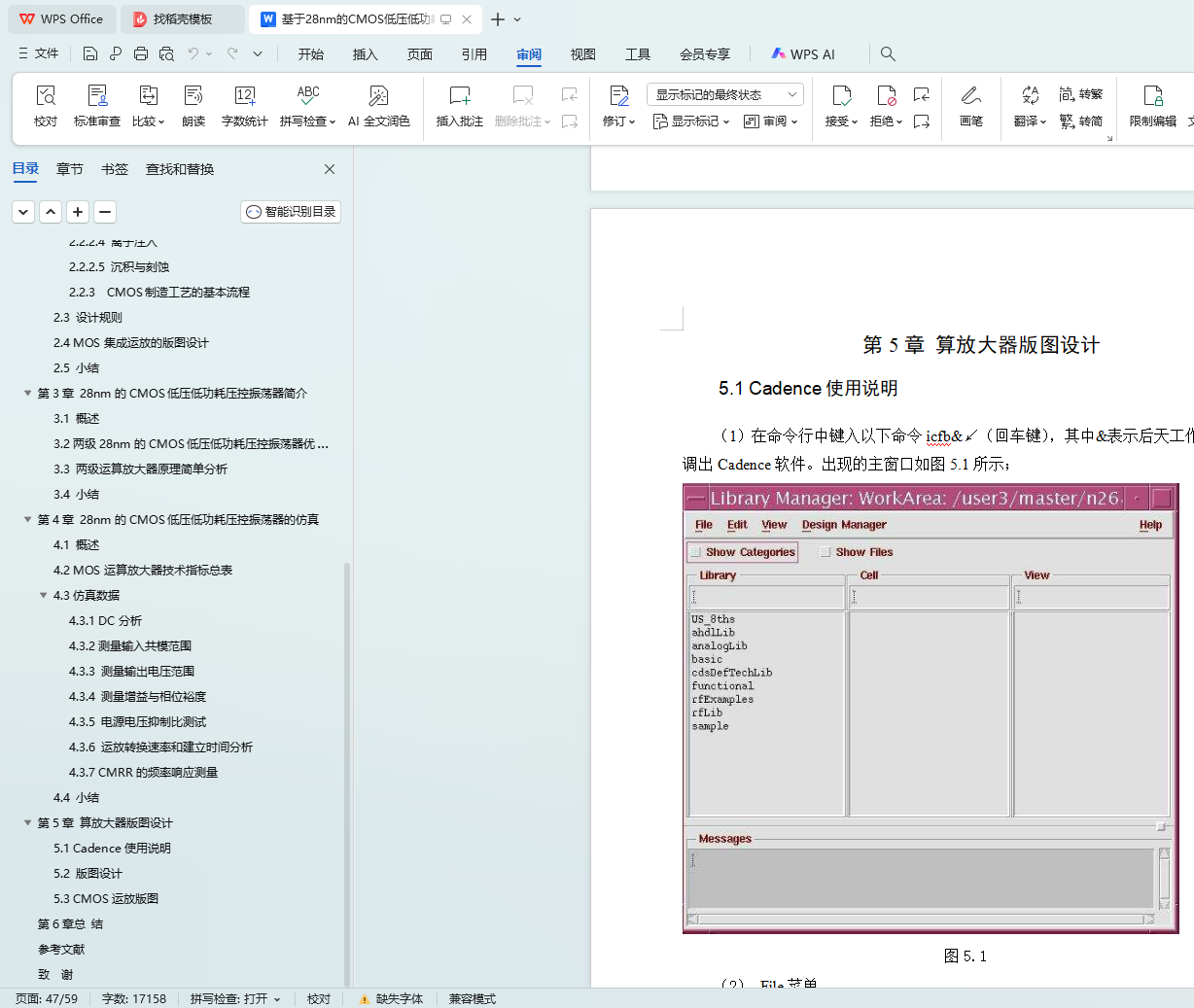
5.1 Cadence使用说明
5.2 版图设计
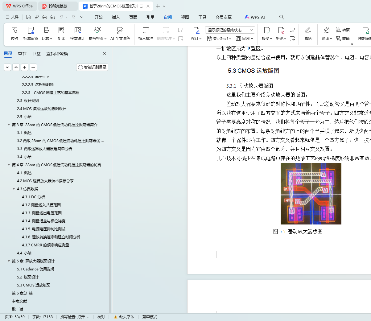
5.3 CMOS运放版图
第6章 总 结
参考文献
致谢词